Integration of nano- and micro-structured materials with the tip of optical fibers is one of the integral parts of making lab-on-fiber technology for sensing applications.
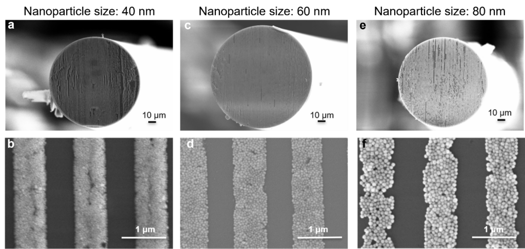
Optical fiber tips have been previously patterned using e-beam lithography, focused ion beam milling, 3D direct laser writing, CVD/PVD processing, direct transfer of nanomaterials from solutions, and wet-transfer of 2D materials. Some of these methods have good spatial resolution but low throughput, others have high throughput but don’t provide the flexibility of deterministic patterning. Here, we demonstrate a low-cost and high-throughput method to pattern optical fiber tips with deterministic placement of nanoparticles.
We use gold nanoparticles deposited PDMS substrates as soft stamps to transfer the gold nanoparticle patterns on optical fiber tips. The gold nanoparticle patterns attach to the fiber tip due to Van der Waals force. Figures show scanning electron microscope images of optical fiber tips functionalized with patterns of gold nanoparticles with different diameters arranged with a periodicity of 1500 nm. The details can be found here on https://doi.org/10.1364/AO.492232 and https://doi.org/10.1364/FIO.2022.JTu4B.9


0 Comments